Computer technology is ????? ?????? ????no strange to acronyms: CPU, GPU, RAM, SSD, BIOS, CD-ROM, to name but a few. Ever so often, new ones appear on the scene, as part of the never-ending quest to improve the features and capabilities of our computing devices.
Today's focus will be on explaining popular processor instruction set extensions MMX, SSE, and AVX and see whether these are cool features to have or just pointless marketing gimmicks.
The oh-so simple early days
Let's start this explainer by heading back in time, to the mid 1980s. The CPU market was quite similar to how it is now, with Intel holding the largest share of sales, but facing stiff competition from AMD. Home computers, such as the Commodore 64, were using basic 8-bit processors, whereas the desktop PC was beginning to shift from 16-bit to 32-bit chips.
The numbers refer to the size of the data values that could be mathematically processed, with larger values helping to give better precision and capability. It also defines the size of the general purpose registers in the chip: tiny amount of memory, used to store the working data.
Such CPUs were also scalar and integer in nature – but what exactly does this mean? Scalar is where any math operation takes place on just single data values: it's typically described as being SISD (single instruction, single data).
So an instruction to add two data values together, just gets processed for those two numbers. If you want to do something like add the same number to a group of 16 numbers, then you'd need to issue 16 sets of instructions to do so. Not great, but that was the limitation of such processors back then.
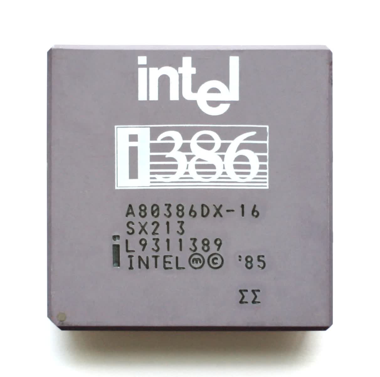
Integer is the mathematical term for a whole number, such as 8 or -12. The likes of Intel's 80386SX processor had no innate ability to add, say, 3.80 and 7.26 – these kinds of numbers are called floats (short for floating point). To crunch them, you needed another processor, such as the 80387SX, and a separate instruction set – the list of commands that tells the CPU what to do.
For CPUs of that time, x86instructions were for integer calculations and x87for float; today, we use the term x86 to cover both of them, because it all gets done by the same chip.
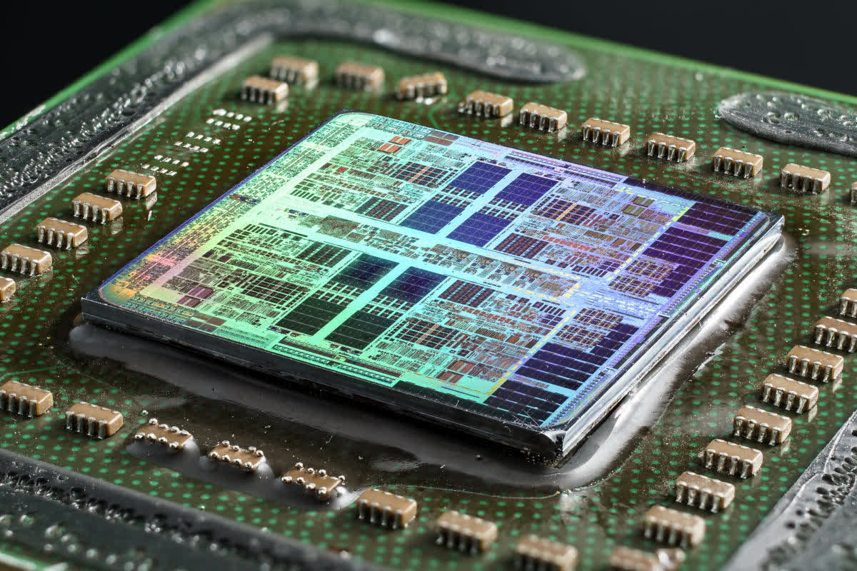
Generally known as co-processors, the use of separate processors for handling integer and float operations was the norm until Intel released the 80486: their first desktop CPU that had an integrated floating point unit (FPU).
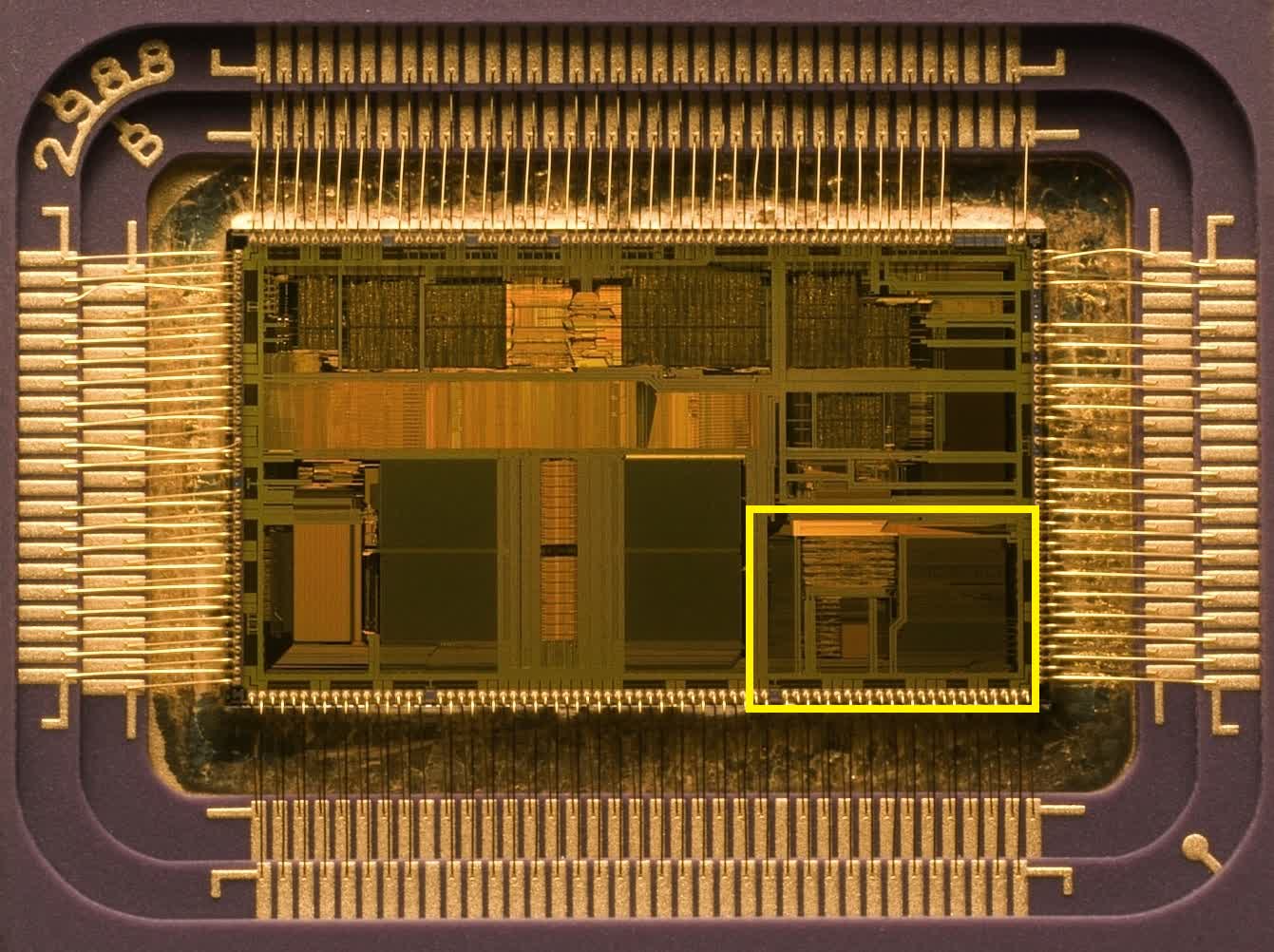
As the image above shows, it took up quite a bit of the processor's overall size, but the performance benefits of having it packaged inside were enormous.
The whole setup was still scalar, though, and it remained the case with the 80486's successor: the original Intel Pentium.
Well, that was the case until 3 years after the release of that particular CPU line. In October 1996, Intel launched the 'Pentium with MMXtechnology'.
V is for vectors, MMX is for...?
In the world of mathematics, numbers can be grouped together into sets of varying shapes and sizes – one particular grouping is called a vector. The best way to think of these is a list of values, running horizontally or vertically. What MMX technology brought to the CPU world was the ability to do vector math.
It was pretty limited to begin with, though, as it was only available for integers. The system actually used the registers dedicated for the FPU to do this, so programmers wanting to fire up some MMX instructions would have to bear in mind that any float calculations couldn't be done at the same time.
The Pentium's FPU had registers that were 64-bits in size, and for MMX operations, each one could be packed with two 32-bit, four 16-bit, or eight 8-bit integers. It's these groups of numbers that are the vectors, and every instruction issued to be processed on them would be carried out on all values in the group.
This type of system is called SIMD (single instruction, multiple data) and marked the big step forwards in the capabilities of CPUs used in desktop PCs.
So what applications benefit from using such a system? Pretty much anything that involves doing the same calculation to groups of numbers, but most notably some of the processing duties in handling 3D graphics, multimedia, and general signals.
For example, MMX could be used to speed up matrix multiplication in vertex processing, or the blending of two video feeds in chroma keying or alpha compositing.
Unfortunately, the uptake on the use of MMX was pretty slow, due to its negative impact of floating point performance. AMD partly fixed this issue by creating their own version of it, called 3DNow! about two years after MMX appeared – it offered more SIMD instructions and could handle floating point numbers, too, but it also suffered from a lack of uptake by programmers.
Oh, and the name? MMX doesn't stand for anything, according to Intel!
Easy as SSE
Matters improved in 1999, with the launch of Intel's Pentium III processor. Its shiny vector feature came in the form of SSE(Streaming SIMD Extensions); this time round there was an extra set of eight 128-bit registers, separate to those in the FPU, and a stack of extra instructions that could handle floats.
The use of the separate registers meant that the FPU was no longer tied down so much, although the Pentium III was unable to issue SSE instructions at the same time as FP ones. The new feature also only supported one data type in the registers: four 32-bit floats.
But the move to offer floating point SIMD instructions enabled the scope for greater performance in applications such as video encoding/decoding, image and audio processing, file compression, and many others.
An updated version, SSE2, appeared in 2001 with the Pentium 4, and this time the data type support was much better: four 32-bit or two 64-bit floats, as well as sixteen 8-bit, eight 16-bit, four 32-bit, or two 64-bit integers. The MMX registers remained in the processor, but all MMX and SSE operations could be made to place using the separate 128-bit SSE registers.
SSE3 came to life in 2003, sporting more instructions and the ability to carry out some math between values residing in the same register.
The Intel Core architecture arrived 3 years later, which brought another revision of the SIMD technology (SSSE3 - Supplemental SSE) with the final version, SSE4, saying hello later in the same year.
The minor update to that version was released with the Nehalem range of Core processors in 2008, with Intel calling it SSE4.2 (so the original version became known as SSE4.1). None of the updates brought any changes to the registers, but more instructions were brought to the table, opening up the range of math and logic operations that could take place.
AMD had proposed a further revision, SSE5, but instead chose to split it up into three separate extensions, one of which would go on to cause a few headaches – more on this in a moment.
By the end of 2008, both Intel and AMD were fielding CPUs that could handle MMX through to SSE4.2 sets of instructions, and many applications (mostly games)were starting to requirethese features in order to run.
Time for new letters
2008 was also the year that Intel announced that they were working on a significant update to their SIMD setup and in 2011, the Sandy Bridge range of CPUs were launched, featuring AVX(Advanced Vector Extensions).
Everything was doubled in number: twice as many vector registers, and twice the size.
The sixteen 256-bit registers could only take eight 32-bit or four 64-bit float numbers, so it was a little more restrictive than SSE in terms of data formats, but that instruction set was still available. By this time, software support for CPU vector operations were well established, from the fundamental world of compilers, through to complex applications.
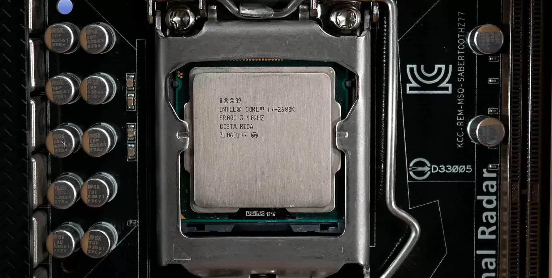
And for good reason: the likes of the Core i7-2600K, running at 3.8 GHz, could potentially churn out over 230 GFLOPS (billion floating point operations per second), when doing AVX instructions – not bad for a relatively small addition to the overall CPU's die size.
Or it would be, if it actually ran at 3.8 GHz. Part of the problem of using AVX was that the load on the chip was so high that Intel had them automatically decrease the clocks in this mode, by around 20%, to keep the power consumption and heat levels down. Unfortunately, this is the price that must be paid to do any SIMD work in a modern CPU.
Another enhancement offered with AVX was the ability to work with three values at a time. In all versions of SSE, operations took place between two values, with the answer then replacing one of them in the register. When doing SIMD instructions, AVX keeps the original values safe and stores the result in a separate register.
The sequel, AVX2 was launched with the Haswell architecture of 4th-gen Core processors in 2013, and it was a significant update thanks to the inclusion of another extension: FMA(fused multiply-accumulate).
Although this was a separate feature to AVX2, the ability to issue one instruction that would then carry out two operations was hugely beneficial for applications doing vector or matrix math, although it worked on scalar operations as well.
However, Intel's FMA extension was different to AMD's; so much so, they're entirely incompatible. This is because Intel's FMA is a three operand system, i.e. it works with 3 separate values – this can be in the form of 2 source numbers and a separate answer, or 3 source values and an answer that replaces one of them.
AMD's is four operand, so it's possible to do math on 3 numbers and not have to write the answer over one of them. While FMA4 is mathematically better than FMA3, the implementation of it is a little more complex, both in terms of programming and integrating the feature into the processor.
AVX-512: a step too far?
As AVX2 just started making its rounds in the CPU market, Intel were already laying down plans for its successor, AVX-512, and the general theme would be 'more, lotsmore.' Not only would there be twice as many registers again, they'd also double in size, and there would be a stack of new instructions and legacy support.
The first batch of chips to wave the AVX-512 feature set in the air was the Xeon Phi 7200 series – the second generation of Intel's hulking many coreprocessors, targeted at the world of supercomputers.
Unlike its previous iterations, the new vector instruction set consisted of 19 subsets: a core foundation, AVX-512F, that had to be offered to be compliant, and then a raft of very specific ones. These extra sets cover operations such as reciprocal math, integer FMA, or convolution neural network algorithms.
Initially, AVX-512 was just the preserve of Intel's biggest chips, aimed at workstations and servers, but now their recent Ice Lake and Tiger Lake architectures offer it, too. Yes, that's right: you can buy a lightweight laptop with a processor sporting 512-bit vector units.
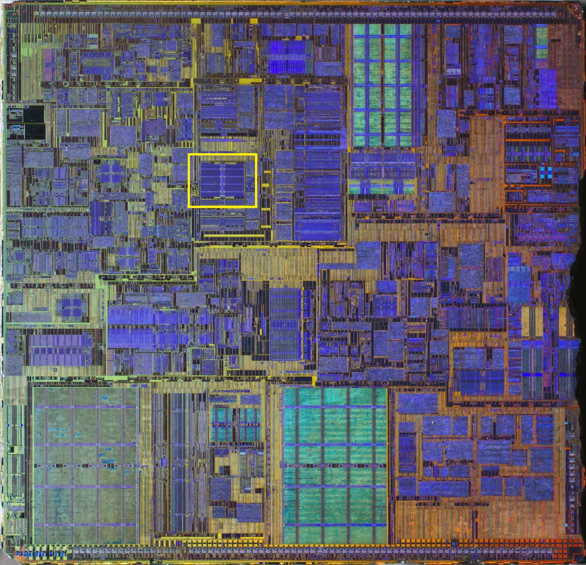
This might seem like a good thing, but that's possibly not the case, depending on your point of view. The registers in a CPU are typically all grouped together in the die, in what's known as a register file, as highlighted in the image of a dual core Intel Skylake chip below.
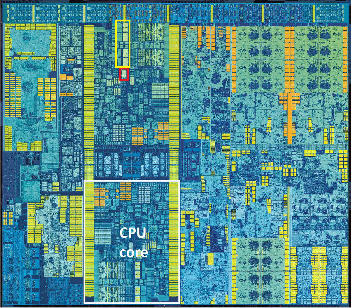
The yellow box highlights the vector register file; the red box is the most likely location of the integer register file. Notice how much larger the vector one is? Skylake uses 256-bit registers for AVX2, so for the same die scale, AVX-512 registers would be fourtimes larger – 2 times for the doubling of the bits and another 2 times for the doubling of the register count.
Does a small chip, designed to be as small as possible for the mobile market, really need to use that much space for vector registers? While it's not a large portion of each core's footprint, every square millimetre counts when it comes to making the best use of the available space.
And given that the use of AVX, in any form, results in the clocks being automatically decreased, the use of AVX-512 on such platforms would almost certainly be worse than using any of its predecessors, as it's even more demanding of power when running.
But it's not just in small mobile CPUs that AVX-512 presents issues. Developers writing code to run on workstations and servers, that will really benefit from using vector extensions, will need to create multiple versions. This is because not all AVX-512 CPUs offer the same instruction sets.
For example, the IFMA set (integer fused multiply-accumulate) is only available on Cannon, Ice, and Tiger Lake CPUs – processors using Cooper and Cascade Lake architectures don't offer this, despite being workstation/server products.
It's worth noting that AMD doesn't offer support for AVX-512 and has no plans to do so. It sees the task of handling large vector calculations as the preserve of the GPU, just as Nvidia does, and both have released products specifically for such roles.
What's next?
The additional capability of CPUs to handle vector math all those years ago marked a significant step forward. Today's processors are extremely capable, offering a mass of instruction sets to handle integer and floating point operations for scalar, vector, and matrix data.
In the case of the last two data types, CPUs now compete directly against GPUs – the world of 3D graphics is all about SIMD, vectors, floats, etc. and the development of graphics accelerators has been meteoric. At the beginning of the last decade, you could get a GPU that could carry out almost 800 billion SIMD instructions per second, for less than $500.
That's greater than even the very best of desktop CPUs can handle now, but they're not designed to be brilliant at every role – they need to handle very generalized code, that's often not very repetitive or easily parallelized. So it's best to think of a CPU's SIMD capability as a handy extra, rather than something that's super important.
But the rise of the GPU does mean that CPUs don't have to sport very big vector units; this is almost certainly why AMD hasn't looked to develop their own successor to AVX2 (an extension they've had in their chips since 2015). Let's also not forget how next-gen CPUs may look more like mobile SoCs with dedicated silicon for certain types of tasks. Intel, on the other hand, seem to be keen on rolling out AVX-512 to as many products as possible.
So will we see an AVX-1024? Probably not, or at the very least, not for a good many years. Instead, Intel are more likely to offer additional instruction subsets for AVX-512, to improve its flexibility, and leave raw SIMD performance to their newly developed GPU line.
SSE and AVX are now an integral part of the software scene: Adobe Photoshop requires CPUs to support SSE4.2, as a minimum; machine learning API TensorFlow demands AVX support in CPUs; Microsoft Teams can only do background video effects is AVX2 is available.
That only means these are not going away soon, despite the SIMD power of a GPU, but hopefully when the next generation of vector extensions comes out, we'll be treated to another dayglo advert for them.